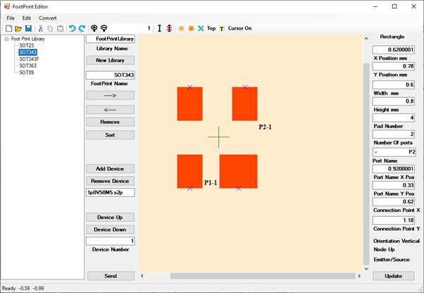
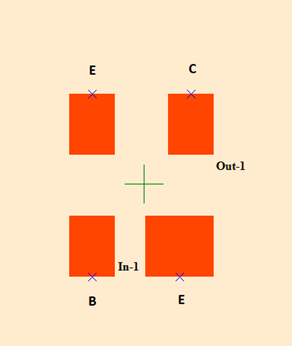
Using the matched transistor in Figure 1 open the Footprint window. In the Footprint window select the SOT343 footprint and click the Right arrow button to display the footprint. Click the Add Device button and select the S-parameter data for the transistor that was used in Figure 1 this was 1p0V50M5.s2p. Change the name of the pads from In-1 and Out-1 to P1 and P2 respectively, by selecting P1 and entering 1 in the Device number textbox and clicking the Update button. Similarly for Out-1, select P2 and 1 in the Device number textbox, Figure 2. Then click the Send button to send it to the Parts window.
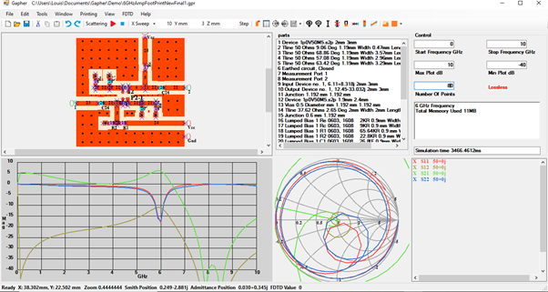
In the Home window remove device footprint and place the SOT343 footprint and rearrange the transmission lines as in Figure 3. The emitter, base and collector of the transistor are shown in Figure 4.
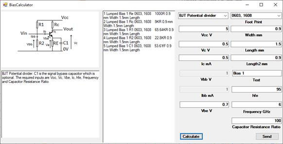
The S-parameter data used were for a BJT biased at VCE=0.5V, Ic=0.5mA and hfe=95. Opening the Bias Calculator in the Window menu and selecting the “BJT Potential Divider”, the above values are entered in the appropriate text boxes with Vc=5V, Vbe=0.7V, frequency=6GHz and 0603,1608 for the footprint and click the Calculate button as in Figure 5.
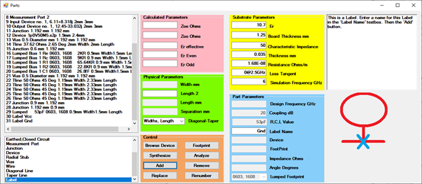
Clicking the Send button will send the parts to the Home and Parts window. Add a 0.5mm Via to the parts and 5 short microstrip lines for the connection of the lumped components. Also add a DC blocking capacitor of 53pF, this can be calculated from , where f is the frequency 6GHz and R the resistance 0.5 Ohms was used, which is 100 times smaller than the microstrip line impedance, and a Vcc and Gnd Label, Figure 6. The footprint for the transistor has two pins for the emitter, therefore the there will have to be a resistor and a capacitor at each pin. These components will be in parallel. The resistance of 1K Ohm will have to be doubled and the capacitance halved. This is done by clicking on the part in the part window, modifying its parameters and clicking the Replace button. Add a Vcc and Gnd label. Place the parts according to the circuit diagram in the Bias Calculator.
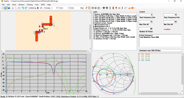
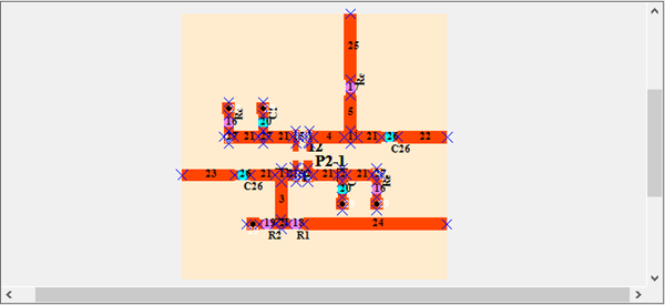
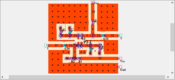
In Figure 7 the bias components are added as in circuit diagram in Figure 5. The microstrip lines 22, 23, 24 and 25 have been stretched to the end of the board using the Stretch line button.
Add copper pour to the entire board by clicking on the Copper Pour button. While in the copper pour board add some vias using the multiple vias selection, here the space of the vias was 2mm by 2mm. Some 0.25mm vias were added singularly on the finer copper pour trace. Finally add the Labels to the microstrip lines to makes it easier to recognise the external connections. The final circuit in Figure 8.
The circuit can be simulated with all the added bias components to confirm the circuit still performs in the required manor, Figure 9.