Microwave and Radio Frequency simulation software
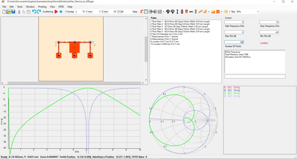
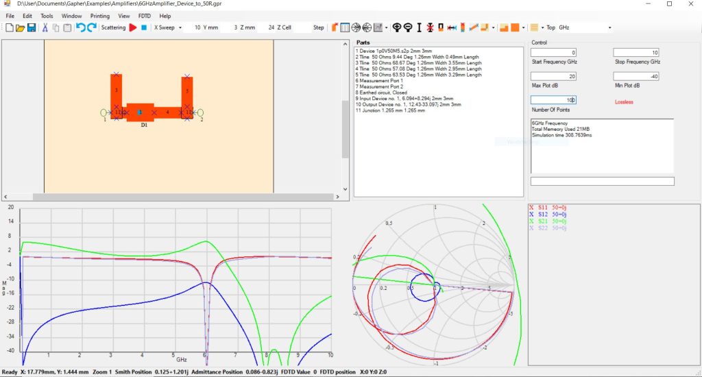
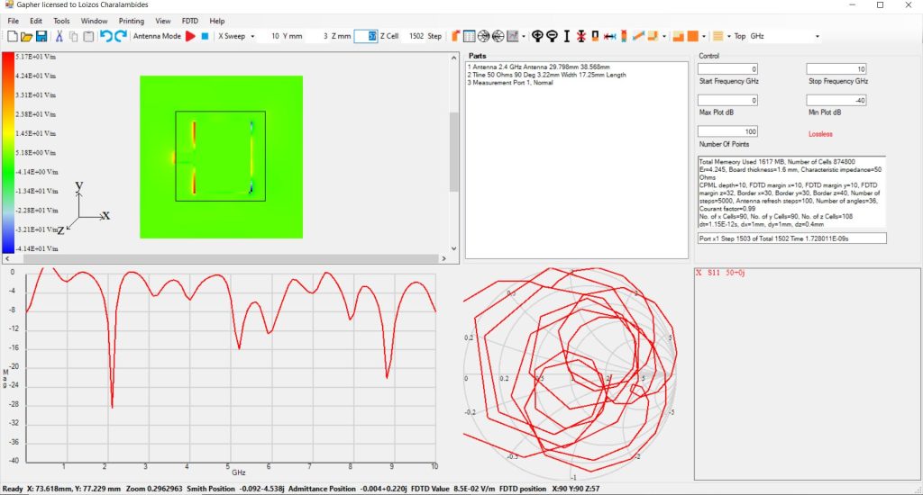
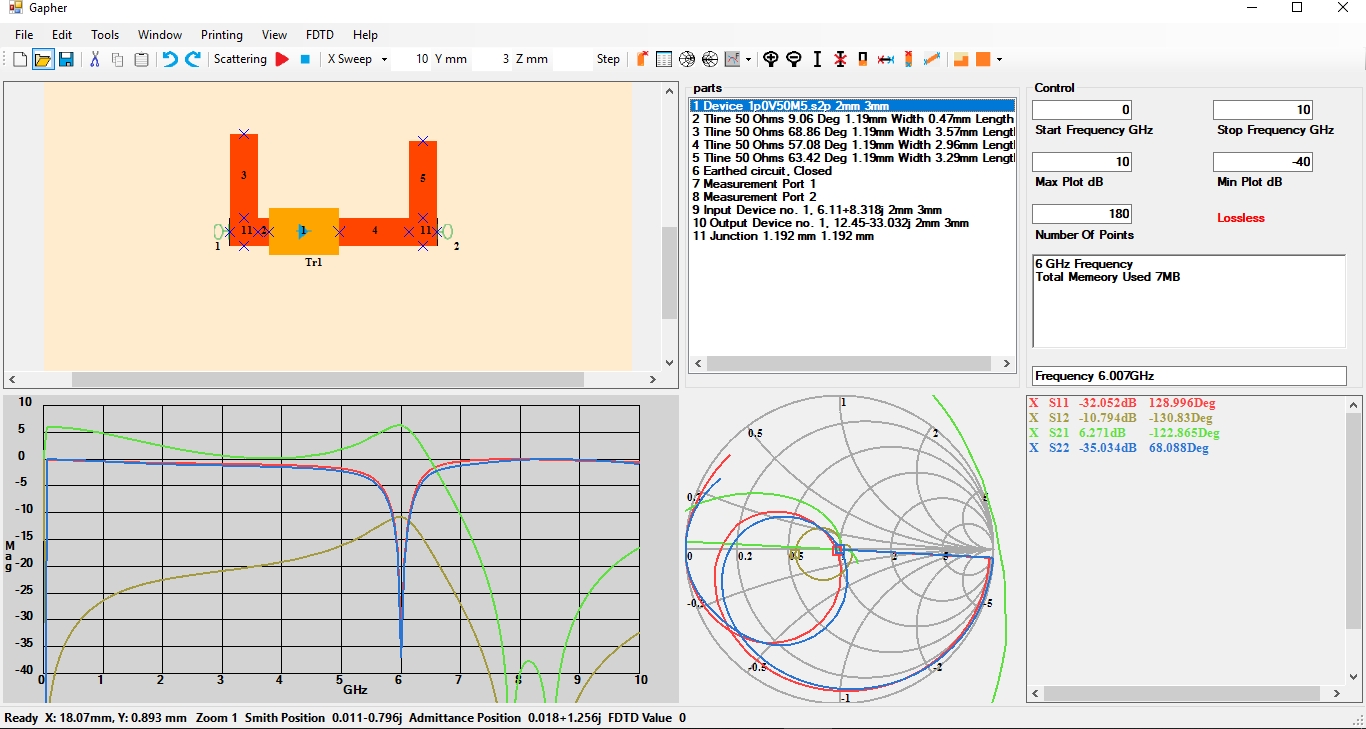
Gapher is a Radio Frequency and Microwave simulation software. It has a scattering parameter engine for designing circuits and an electromagnetic Finite Difference Time Domain engine for electromagnetic simulation. These two engines are integrated together in one seamless package.
It is intended for students and hobbyists as a computer aided design program and is competitively priced.
It allows users do design microwave circuits quickly and export their work in a Gerber file, to be manufactured, or printed film for the manufacture of a PCB in house.
Filters, amplifiers, couplers, patch antenna etc. can be easily be designed using Gapher. They can be joined together to form bigger circuits.
Match and simulate microwave circuits, simply and easily. Produce masks for PCB production in house.